|
Product Details:
|
| Product Name: | Mosfet Power Transistor | APPLICATION: | Power Management |
|---|---|---|---|
| FEATURE: | Excellent RDS(on) | Power Mosfet Transistor: | Enhancement Mode Power MOSFET |
| Model Number: | 5N20DY | ||
| High Light: | n channel mosfet transistor,high voltage transistor |
||
5N20D / Y 200V N-Channel Enhancement Mode MOSFET
The AP50N20D uses advanced trench
technology to provide excellent RDS(ON) and low gate charge .
The complementary MOSFETs may be used to form a level shifted high side switch, and for a host of other
![]()
![]()
FEATURES
VDS =200V,ID =5A
RDS(ON) <520mΩ @ VGS=4.5V
Application
Load switching
Hard switched and high frequency circuits Uninterruptible power supply
![]()
| Product ID | Pack | Marking | Qty(PCS) |
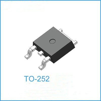
| 5N20D | TO-252 | 5N20D | 3000 |
| 5N20Y | TO-251 | 5N20Y | 4000 |
Note: Pin Assignment: G: Gate D: Drain S: Source
ABSOLUTE MAXIMUM RATINGS (TC = 25°С, unless otherwise specified)
| Parameter | Symbol | Limit | Unit |
| Drain-Source Voltage | VDS | 200 | V |
| Gate-Source Voltage | VGS | ±20 | V |
| Drain Current-Continuous | ID | 5 | A |
| Drain Current-Pulsed (Note 1) | IDM | 20 | A |
| Maximum Power Dissipation | PD | 30 | W |
| Operating Junction and Storage Temperature Range | TJ,TSTG | -55 To 150 | ℃ |
Notes: 1. Absolute maximum ratings are those values beyond which the device could be permanently damaged.
Absolute maximum ratings are stress ratings only and functional device operation is not implied.
4. Repetitive Rating: Pulse width limited by maximum junction temperature.
5. L = 84mH, IAS =1.4A, VDD = 50V, RG = 25 Ω Starting TJ = 25°C
6. ISD ≤ 2.0A, di/dt ≤200A/μs, VDD ≤BVDSS, Starting TJ = 25°C
| Thermal Resistance,Junction-to-Ambient (Note 2) | RθJA | 4.17 | ℃/W |
ELECTRICAL CHARACTERISTICS (TJ = 25°С, unless otherwise specified)
| Parameter | Symbol | Condition | Min | Typ | Max | Unit |
| Off Characteristics | ||||||
| Drain-Source Breakdown Voltage | BVDSS | VGS=0V ID=250μA | 200 | - | - | V |
| Zero Gate Voltage Drain Current | IDSS | VDS=200V,VGS=0V | - | - | 1 | μA |
| Gate-Body Leakage Current | IGSS | VGS=±20V,VDS=0V | - | - | ±100 | nA |
| On Characteristics (Note 3) | ||||||
| Gate Threshold Voltage | VGS(th) | VDS=VGS,ID=250μA | 1.2 | 1.7 | 2.5 | V |
| Drain-Source On-State Resistance | RDS(ON) | VGS=10V, ID=2A | - | 520 | 580 | mΩ |
| Forward Transconductance | gFS | VDS=15V,ID=2A | - | 8 | - | S |
| Dynamic Characteristics (Note4) | ||||||
| Input Capacitance | Clss |
VDS=25V,VGS=0V, F=1.0MHz |
- | 580 | - | PF |
| Output Capacitance | Coss | - | 90 | - | PF | |
| Reverse Transfer Capacitance | Crss | - | 3 | - | PF | |
| Switching Characteristics (Note 4) | ||||||
| Turn-on Delay Time | td(on) |
VDD=100V, RL=15Ω VGS=10V,RG=2.5Ω |
- | 10 | - | nS |
| Turn-on Rise Time | tr | - | 12 | - | nS | |
| Turn-Off Delay Time | td(off) | - | 15 | - | nS | |
| Turn-Off Fall Time | tf | - | 15 | - | nS | |
| Total Gate Charge | Qg |
VDS=100V,ID=2A, VGS=10V |
- | 12 | nC | |
| Gate-Source Charge | Qgs | - | 2.5 | - | nC | |
| Gate-Drain Charge | Qgd | - | 3.8 | - | nC | |
| Drain-Source Diode Characteristics | ||||||
| Diode Forward Voltage (Note 3) | VSD | VGS=0V,IS=2A | - | - | 1.2 | V |
| Diode Forward Current (Note 2) | IS | - | - | 5 | A | |
Notes: 1. Pulse Test : Pulse width ≤ 300µs, Duty cycle ≤ 2%.
![]()
![]()
![]()
![]()
![]()
Contact Person: David