|
Product Details:
|
| Model Number: | 12N60 | Product Name: | Mosfet Power Transistor |
|---|---|---|---|
| APPLICATION: | Power Management | FEATURE: | Excellent RDS(on) |
| Power Mosfet Transistor: | Enhancement Mode Power MOSFET | Type: | N Channel Mosfet Transistor |
| High Light: | n channel mosfet transistor,high voltage transistor |
||
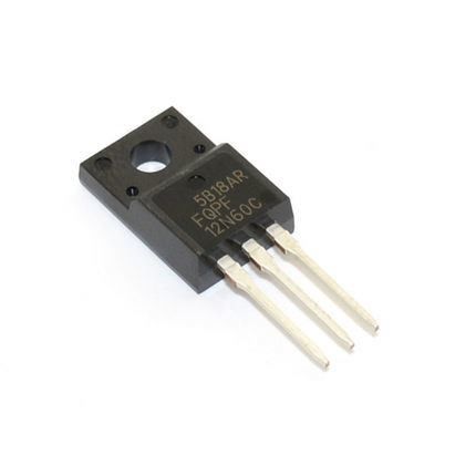
OEM N Channel Mosfet Transistor , Small Mosfet Power Switch Enhancement Mode
N Channel Mosfet Transistor DESCRIPTION
The UTC 12N60-C is a high voltage power MOSFET designed to have better characteristics, such as fast switching time, low gate charge, low on-state resistance and high rugged avalanche characteristics. This power MOSFET is usually used in high speed switching applications of switching power supplies and adaptors.
![]()
N Channel Mosfet Transistor FEATURES
* RDS(ON) < 0.7 Ω @ VGS = 10 V, ID = 6.0 A
* Fast switching capability
* Avalanche energy tested
* Improved dv/dt capability, high ruggedness
![]()
| Ordering Number | Package | Pin Assignment | Packing | |||
| Lead Free | Halogen Free | 1 | 2 | 3 | ||
| 12N60L-TF1-T | 12N60G-TF1-T | TO-220F1 | G | D | S | Tube |
| 12N60L-TF3-T | 12N60G-TF3-T | TO-220F | G | D | S | Tube |
Note: Pin Assignment: G: Gate D: Drain S: Source
![]()
ABSOLUTE MAXIMUM RATINGS (TC = 25°С, unless otherwise specified)
| PARAMETER | SYMBOL | TEST CONDITIONS | MIN | TYP | MAX | UNI T | |
| OFF CHARACTERISTICS | |||||||
| Drain-Source Breakdown Voltage | BVDSS | VGS=0V, ID=250μA | 600 | V | |||
| Drain-Source Leakage Current | IDSS | VDS=600V, VGS=0V | 1 | μA | |||
| Gate- Source Leakage Current | Forward | IGSS | VGS=30V, VDS=0V | 100 | nA | ||
| Reverse | VGS=-30V, VDS=0V | -100 | nA | ||||
| ON CHARACTERISTICS | |||||||
| Gate Threshold Voltage | VGS(TH) | VDS=VGS, ID=250μA | 2.0 | 4.0 | V | ||
| Static Drain-Source On-State Resistance | RDS(ON) | VGS=10V, ID=6.0A | 0.7 | Ω | |||
| DYNAMIC CHARACTERISTICS | |||||||
| Input Capacitance | CISS |
VGS=0V, VDS=25V, f =1.0 MHz |
1465 | pF | |||
| Output Capacitance | COSS | 245 | pF | ||||
| Reverse Transfer Capacitance | CRSS | 57 | pF | ||||
| SWITCHING CHARACTERISTICS | |||||||
| Total Gate Charge (Note 1) | QG | VDS=50V, ID=1.3A, IG=100μA VGS=10V (Note 1,2) | 144 | nC | |||
| Gate-Source Charge | QGS | 10 | nC | ||||
| Gate-Drain Charge | QGD | 27 | nC | ||||
| Turn-On Delay Time (Note 1) | tD(ON) |
VDD =30V, ID =0.5A, RG =25Ω, VGS=10V (Note 1,2) |
81 | ns | |||
| Turn-On Rise Time | tR | 152 | ns | ||||
| Turn-Off Delay Time | tD(OFF) | 430 | ns | ||||
| Turn-Off Fall Time | tF | 215 | ns | ||||
| DRAIN-SOURCE DIODE CHARACTERISTICS AND MAXIMUM RATINGS | |||||||
| Maximum Continuous Drain-Source Diode Forward Current | IS | 12 | A | ||||
|
Maximum Pulsed Drain-Source Diode Forward Current |
ISM | 48 | A | ||||
| Drain-Source Diode Forward Voltage | VSD | VGS=0 V, IS=6.0 A | 1.4 | V | |||
| Reverse Recovery Time | trr |
VGS=0 V, IS=6.0 A, dIF/dt=100 A/μs (Note 1) |
336 | ns | |||
| Reverse Recovery Charge | Qrr | 2.21 | μC | ||||
Notes: 1. Absolute maximum ratings are those values beyond which the device could be permanently damaged.
Absolute maximum ratings are stress ratings only and functional device operation is not implied.
4. Repetitive Rating: Pulse width limited by maximum junction temperature.
5. L = 84mH, IAS =1.4A, VDD = 50V, RG = 25 Ω Starting TJ = 25°C
6. ISD ≤ 2.0A, di/dt ≤200A/μs, VDD ≤BVDSS, Starting TJ = 25°C
ELECTRICAL CHARACTERISTICS (TJ = 25°С, unless otherwise specified)
| Parameter | Symbol | Condition | Min | Typ | Max | Unit |
| Off Characteristics | ||||||
| Drain-Source Breakdown Voltage | BVDSS | VGS=0V ID=250μA | 100 | 110 | - | V |
| Zero Gate Voltage Drain Current | IDSS | VDS=100V,VGS=0V | - | - | 1 | μA |
| Gate-Body Leakage Current | IGSS | VGS=±20V,VDS=0V | - | - | ±100 | nA |
| On Characteristics (Note 3) | ||||||
| Gate Threshold Voltage | VGS(th) | VDS=VGS,ID=250μA | 1.2 | 1.8 | 2.5 | V |
| Drain-Source On-State Resistance | RDS(ON) | VGS=10V, ID =8A | 98 | 130 | m Ω | |
| Forward Transconductance | gFS | VDS=25V,ID=6A | 3.5 | - | - | S |
| Dynamic Characteristics (Note4) | ||||||
| Input Capacitance | Clss |
VDS=25V,VGS=0V, F=1.0MHz |
- | 690 | - | PF |
| Output Capacitance | Coss | - | 120 | - | PF | |
| Reverse Transfer Capacitance | Crss | - | 90 | - | PF | |
| Switching Characteristics (Note 4) | ||||||
| Turn-on Delay Time | td(on) |
VDD=30V,ID=2A,RL=15Ω VGS=10V,RG=2.5Ω |
- | 11 | - | nS |
| Turn-on Rise Time | tr | - | 7.4 | - | nS | |
| Turn-Off Delay Time | td(off) | - | 35 | - | nS | |
| Turn-Off Fall Time | tf | - | 9.1 | - | nS | |
| Total Gate Charge | Qg |
VDS=30V,ID=3A, VGS=10V |
- | 15.5 | nC | |
| Gate-Source Charge | Qgs | - | 3.2 | - | nC | |
| Gate-Drain Charge | Qgd | - | 4.7 | - | nC | |
| Drain-Source Diode Characteristics | ||||||
| Diode Forward Voltage (Note 3) | VSD | VGS=0V,IS=9.6A | - | - | 1.2 | V |
| Diode Forward Current (Note 2) | IS | - | - | 9.6 | A | |
| Reverse Recovery Time | trr |
TJ = 25°C, IF =9.6A di/dt = 100A/μs(Note3) |
- | 21 | nS | |
| Reverse Recovery Charge | Qrr | - | 97 | nC | ||
| Forward Turn-On Time | ton | Intrinsic turn-on time is negligible (turn-on is dominated by LS+LD) | ||||
Essentially independent of operating temperature.Notes: 1. Pulse Test : Pulse width ≤ 300µs, Duty cycle ≤ 2%.
![]()
![]()
Contact Person: Mr. David Lee
Tel: +86 13417075252
Fax: 86-755-83232335