|
Product Details:
|
| Product Name: | Mos Field Effect Transistor | V DSS Drain-Source Voltage: | -100 V |
|---|---|---|---|
| V GSS Gate-Source Voltage: | ±20 V | T J Maximum Junction Temperature: | 175 °C |
| T STG Storage Temperature Range: | -55 To 175 °C | Type: | V Configurations |
| High Light: | logic mosfet switch,mosfet driver using transistor |
||
V Configurations Mos Field Effect Transistor N / P Channel Enhancement Mode
Mos Field Effect Transistor Introduction
MOSFET technology is ideal for use in many power applications, where the low switch on resistance enables high levels of efficiency to be attained.
There is a number of different varieties of power MOSFET available from different manufacturers, each with its own characteristics and abilities.
Many power MOSFETs incorporate a vertical structure topology. This enables high current switching with high efficiency within a relatively small die area. It also enables the device to support high current and voltage switching.
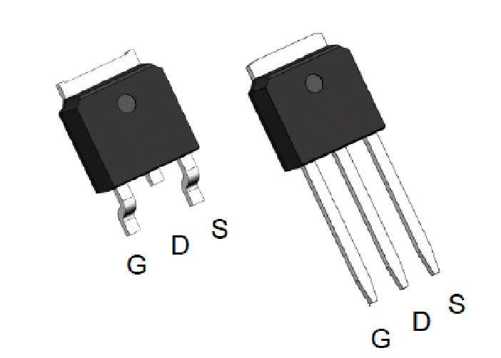
Mos Field Effect Transistor Feature Pin Description
-100V/-10A
R DS(ON) = 187mΩ(typ.)@V GS = -10V
R DS(ON) = 208mΩ(typ.)@V GS = -4.5V
100%Avalanche Tested
Reliable and Rugged
Halogen Free and Green DevicesAvailable
(RoHSCompliant)
Mos Field Effect Transistor Applications
Power Management for Inverter Systems
Ordering and Marking Information
Package Code
D: TO-252-2L U: TO-251-3L
Date Code Assembly Material
YYXXX WW G:Halogen Free
Note: HUAYI lead-free products contain molding compounds/die attach materials and 100% matte tin plateTermi-
Nation finish; which are fully compliant with RoHS. HUAYI lead-free products meet or exceed the lead-Free require-
ments of IPC/JEDEC J-STD-020 for MSL classification at lead-free peak reflow temperature. HUAYI defines “Green”
to mean lead-free (RoHS compliant) and halogen free (Br or Cl does not exceed 900ppm by weight in homogeneous
material and total of Br and Cl does not exceed 1500ppm by weight).
HUAYI reserves the right to make changes, corrections, enhancements, modifications, and improvements to this pr
-oduct and/or to this document at any time without notice
Absolute Maximum Ratings
![]()
Note: * Repetitive rating;pulse width limited by max.junction temperature.
** Limited by T J max , starting T J =25°C , L = 0.5mH , VD=-80V ,V GS =-10V.
Electrical Characteristics (Tc =25°C UnlessOtherwiseNoted)
![]()
Electrical Characteristics (Cont.) (Tc =25°C UnlessOtherwiseNoted)
![]()
Note:*Pulse test,pulsewidth≤ 300us,dutycycle≤ 2%
![]()
Contact Person: David