|
Product Details:
|
| Product Name: | N Channel Mos Field Effect Transistor | Model: | AP10H06S |
|---|---|---|---|
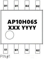
| Pack: | SOP-8 | Marking: | AP10H06S |
| VDSDrain-Source Voltage: | 60V | VGSGate-Sou Rce Voltage: | ±20A |
| High Light: | n channel mosfet transistor,high voltage transistor |
||
AP10H06S N Channel Mos Field Effect Transistor High Frequency
N Channel Mos Field Effect Transistor types
Within the overall arena of power MOSFETs, there are a number of specific technologies that have been developed and addressed by different manufacturers. They use a number of different techniques that enable the power MOSFETs to carry the current and handle the power levels more efficiently. As already mentioned they often incorporate a form of vertical structure
The different types of power MOSFET have different attributes and therefore can be particularly suited for given applications.
N Channel Mos Field Effect Transistor Features
VDS = 60V ID =10A
RDS(ON) < 20mΩ @ VGS=10V
N Channel Mos Field Effect Transistor Application
Battery protection
Load switch
Uninterruptible power supply
Package Marking and Ordering Information
| Product ID | Pack | Marking | Qty(PCS) |
| AP10H06S | SOP-8 | AP10H06S | 3000 |
Absolute Maximum Ratings (TC=25℃unless otherwise noted)
| Parameter | Symbol | Limit | Unit |
| Drain-Source Voltage | VDS | 60 | V |
| Gate-Source Voltage | VGS | ±20 | V |
| Drain Current-Continuous | ID | 10 | A |
| Drain Current-Continuous(TC=100 ℃) | ID (100 ℃) | 5.6 | A |
| Pulsed Drain Current | IDM | 32 | A |
| Maximum Power Dissipation | PD | 2.1 | W |
| Operating Junction and Storage Temperature Range | T J ,T STG | -55 To 150 | ℃ |
| Thermal Resistance,Junction-to-Ambient (Note 2) | RθJA | 60 | ℃/W |
Electrical Characteristics (TC=25℃unless otherwise noted)
| Parameter | Symbol | Condition | Min | Typ | Max | Unit |
| Drain-Source Breakdown Voltage | BV DSS | V GS=0V ID=250μA | 60 | - | V | |
| Zero Gate Voltage Drain Current | IDSS | V DS=60V,V GS=0V | - | - | 1 | μA |
| Gate-Body Leakage Current | IGSS | V GS=±20V,VDS=0V | - | - | ±100 | nA |
| Gate Threshold Voltage | V GS(th) | V DS=V GS,ID=250 μA | 1.0 | 1.6 | 2.2 | V |
|
Drain-Source On-State Resistance |
RDS(ON) |
V GS=10V, ID=8A | - | 15.6 | 20 | mΩ |
| V GS=4.5V, ID=8A | - | 20 | 28 | mΩ | ||
| Forward Transconductance | gFS | V DS=5V,ID=8A | 18 | - | - | S |
| Input Capacitance | Clss |
V DS=30V,V GS=0V, F=1.0MHz |
- | 1600 | - | PF |
| Output Capacitance | Coss | - | 112 | - | PF | |
| Reverse Transfer Capacitance | Crss | - | 98 | - | PF | |
| Turn-on Delay Time | td(on) | - | 7 | - | nS | |
| Turn-on Rise Time |
r t |
- | 5.5 | - | nS | |
| Turn-Off Delay Time | td(off) | - | 29 | - | nS | |
| Turn-Off Fall Time |
f t |
- | 4.5 | - | nS | |
| Total Gate Charge | Qg |
V DS=30V,ID=8A, V GS=10V |
- | 38.5 | - | nC |
| Gate-Source Charge | Qgs | - | 4.7 | - | nC | |
| Gate-Drain Charge | Qgd | - | 10.3 | - | nC | |
| Diode Forward Voltage (Note 3) | V SD | V GS=0V,IS=8A | - | - | 1.2 | V |
| Diode Forward Current (Note 2) | IS | - | - | - | 8 | A |
| Reverse Recovery Time |
rr t |
TJ = 25°C, IF =8A di/dt = 100A/ μs |
- | 28 | - | nS |
| Reverse Recovery Charge | Qrr | - | 40 | - | nC |
Note
1. Repetitive Rating: Pulse width limited by maximum junction temperature.
2. Surface Mounted on FR4 Board, t ≤ 10 sec.
3. Pulse Test: Pulse Width ≤ 300 μs, Duty Cycle ≤ 2%.
4. Guaranteed by design, not subject to production
Attention
1, Any and all APM Microelectronics products described or contained herein do not have specifications that can handle applications that require extremely high levels of reliability, such as life support systems, aircraft's control systems, or other applications whose failure can be reasonably expected to result in serious physical and/or material damage. Consult with your APM Microelectronics representative nearest you before using any APM Microelectronics products described or contained herein in such applications.
2, APM Microelectronics assumes no responsibility for equipment failures that result from using products at values that exceed, even momentarily, rated values (such as maximum ratings, operating condition ranges, or other parameters) listed in products specifications of any and all APM Microelectronics products described or contained herein.
3, Specifications of any and all APM Microelectronics products described or contained here instipulate the performance, characteristics, and functions of the described products in the independent state, and are not guarantees of the performance, characteristics, and functions of the described products as mounted in the customer’s products or equipment. To verify symptoms and states that cannot be evaluated in an independent device, the customer should always evaluate and test devices mounted in the customer’s products or equipment.
4, APM Microelectronics Semiconductor CO., LTD. strives to supply high quality high reliability products. However, any and all semiconductor products fail with some probability. It is possible that these probabilistic failures could give rise to accidents or events that could endanger human lives that could give rise to smoke or fire, or that could cause damage to other property. Whendesigning equipment, adopt safety measures so that these kinds of accidents or events cannot occur. Such measures include but are not limited to protective circuits and error prevention circuits for safe design, redundant design,and structural design.
5,In the event that any or all APM Microelectronics products(including technical data, services) described or contained herein are controlled under any of applicable local export control laws and regulations, such products must not be exported without obtaining the export license from the authorities concerned in accordance with the above law.
6, No part of this publication may be reproduced or transmitted in any form or by any means,electronic or mechanical, including photocopying and recording, or any information storage or retrieval system, or otherwise, without the prior written permission of APM Microelectronics Semiconductor CO., LTD.
Contact Person: David