|
Product Details:
|
| Model Number:: | AP1332GEU-HF | Type:: | Electronic Components |
|---|---|---|---|
| Diode:: | Transistor | IGBT Module:: | High-frequency Tube |
| Inductor:: | LED | D/C:: | Newest |
| High Light: | 2.5A Mosfet Power Transistor,0.35W Mosfet Power Transistor,AP1332GEU-HF Diode Mosfet Transistor |
||
Cheap Factory Price AP1332GEU-HF Please Contact The Business, Is On Same Day Shall Prevail
Description
AP1332 series are from Advanced Power innovated design and silicon process technology to achieve the lowest possible on- resistance and fast switching performance. It provides the designer with an extreme efficient device for use in a wide range of power applications.
Notes:
1.Pulse width limited by Max. junction temperature.
2.Pulse test.
3.Surface mounted on FR4 board, t ≦ 10 sec.
Absolute Maximum Ratings@Tj=25.oC(unless otherwise specified)
| Symbol | Parameter | Rating | Unit |
| VDS | Drain-Source Voltage | 20 | V |
| VGS | Gate-Source Voltage | +8 | V |
| ID@TA=25℃ | Drain Current3, VGS @ 4.5V | 600 | mA |
| ID@TA=70℃ | Drain Current3, VGS @ 4.5V | 470 | mA |
| IDM | Pulsed Drain Current1 | 2.5 | A |
| PD@TA=25℃ | Total Power Dissipation | 0.35 | W |
| TSTG | Storage Temperature Range | -55 to 150 | ℃ |
| TJ | Operating Junction Temperature Range | -55 to 150 | ℃ |
Thermal Data
| Symbol | Parameter | Value | Unit |
| Rthj-a | Maximum Thermal Resistance, Junction-ambient3 | 360 | ℃/W |
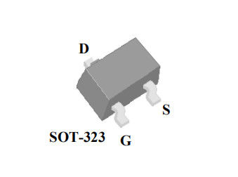
AP1332GEU-H
Electrical Characteristics@Tj=25oC(unless otherwise specified)
| Symbol | Parameter | Test Conditions | Min. | Typ. | Max. | Unit |
| BVDSS | Drain-Source Breakdown Voltage | VGS=0V, ID=250uA | 20 | - | - | V |
| RDS(ON) | Static Drain-Source On-Resistance2 | VGS=4.5V, ID=600mA | - | - | 0.6 | Ω |
| VGS=2.5V, ID=300mA | - | - | 2 | Ω | ||
| VGS(th) | Gate Threshold Voltage | VDS=VGS, ID=250uA | 0.5 | - | 1.25 | V |
| gfs | Forward Transconductance | VDS=5V, ID=600mA | - | 1 | - | S |
| IDSS | Drain-Source Leakage Current | VDS=16V, VGS=0V | - | - | 10 | uA |
| IGSS | Gate-Source Leakage | VGS=+8V, VDS=0V | - | - | +30 | uA |
| Qg | Total Gate Charge |
ID=600mA VDS=16V VGS=4.5V |
- | 1.3 | 2 | nC |
| Qgs | Gate-Source Charge | - | 0.3 | - | nC | |
| Qgd | Gate-Drain ("Miller") Charge | - | 0.5 | - | nC | |
| td(on) | Turn-on Delay Time |
VDS=10V ID=600mA RG=3.3Ω VGS=5V |
- | 21 | - | ns |
| tr | Rise Time | - | 53 | - | ns | |
| td(off) | Turn-off Delay Time | - | 100 | - | ns | |
| tf | Fall Time | - | 125 | - | ns | |
| Ciss | Input Capacitance |
VGS=0V V.DS=10V f=1.0MHz |
- | 38 | 60 | pF |
| Coss | Output Capacitance | - | 17 | - | pF | |
| Crss | Reverse Transfer Capacitance | - | 12 | - | pF |
Source-Drain Diode
| Symbol | Parameter | Test Conditions | Min. | Typ. | Max. | Unit |
| VSD | Forward On Voltage2 | IS=300mA, VGS=0V | - | - | 1.2 | V |
[Shipping]
1. We will ship the items within 2 working days after the payment confirmed.
2. We can ship to you by UPS/DHL/TNT/EMS/FedEx. Please contact us directly and we will use your preferred ways. For the Countries & Regions where EMS cannot deliver, please choose other shipping ways.
3. We are not responsible for any accidents, delays or other issues caused by the forwarder.
4. Any import fees or charges are on the buyer's account
Contact Person: David